Native Block Memory Generator Feature Summary
Memory Types
The Block Memory Generator core uses embedded block RAM to generate five types of
memories:
• Single-port RAM
• Simple Dual-port RAM
• True Dual-port RAM
• Single-port ROM
• Dual-port ROM
For dual-port memories, each port operates independently.
Operating mode, clock frequency, optional output registers, and optional pins are selectable per port.
For Simple Dual-port RAM, the operating modes are not selectable.
Configurable Width and Depth
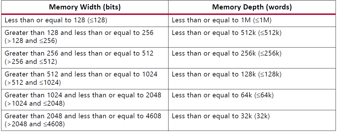
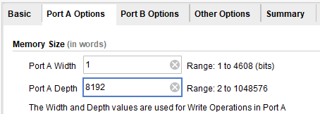
The Block Memory Generator core can generate memory structures from 1 to 4608 bits wide, and at least two locations deep.
The maximum depth of the memory is limited only by the number of block RAM primitives in the target device.
Supports memory sizes up to a maximum of 16 MBytes (byte size 8 or 9) (limited only by memory resources on selected part)
Selectable Port Aspect Ratios
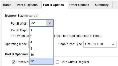
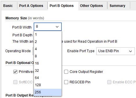
• The A port width might differ from the B port width by a factor of 1, 2, 4, 8, 16, or 32.
• Poart A Width가 1일 때 Port B Width 설정 가능 옵션
• Poart A Width가 8일 때 Port B Width 설정 가능 옵션

Optional Byte-Write Enable
(?) The Block Memory Generator core provides byte-Write support for memory widths which
are multiples of eight (no parity) or nine bits (with parity).
Byte-writes: When using byte-writes, no two data widths can have a ratio greater than 4:1.
Consider a Single-port RAM with a data width of 24 bits, or 3 bytes with byte size of 8 bits.
The Write enable bus, wea, consists of 3 bits. Figure 3-14 illustrates the use of byte-writes,
and shows the contents of the RAM at address 0. Assume all memory locations are
initialized to 0

Optional Output Registers
The Block Memory Generator core provides two optional stages of output registering to
increase memory performance.
The output registers can be chosen for port A and port B separately. The core supports embedded block RAM registers as well as registers implemented in the FPGA general interconnect.
Optional Pipeline Stages
The core provides optional pipeline stages within the MUX, available only when the registers at the output of the memory core are enabled and only for specific configurations. For the available configurations, the number of pipeline stages can be 1, 2, or 3.
Optional Enable Pin
When deasserted, no Read, Write, or reset operations are performed on the respective port.
리셋도 동작하지 않는다.
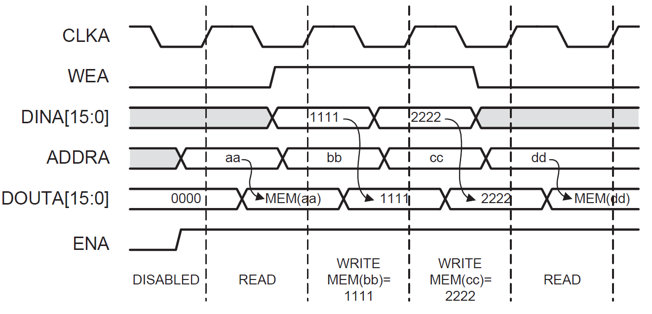
The Simple Dual-port RAM
• Write access to the memory is allowed through port A.
• Read access is allowed through port B.
The True Dual-port RAM
• Read and Write accesses to the memory are allowed on either port.
Operating Mode
The operating modes have an effect on the relationship between the A and B ports when the A and B port addresses have a collision (?). For detailed information about collision behavior, see Collision Behavior, page 51. For more information about operating modes, see the block RAM section of the user guide specific to the device family.
Write First Mode: 읽고 쓰기가 동시에 이루어질 때 우선 쓰고 다음에 읽는다.
Note: The WRITE_FIRST operation is affected by the optional byte-Write feature. It is also affected by the optional Read-to-Write aspect ratio feature.
Read First Mode: 읽고 쓰기가 동시에 이루어질 때 우선 읽고 다음에 쓴다.
In READ_FIRST mode, data previously stored at the Write address appears on the data output
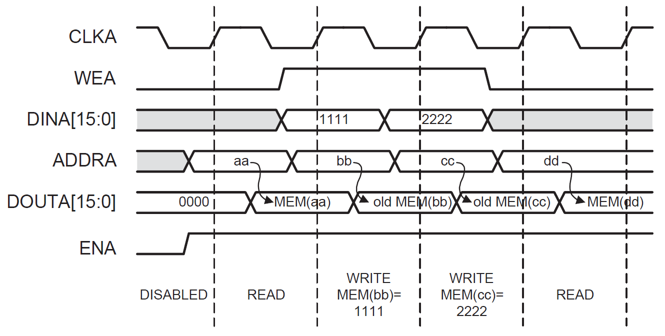
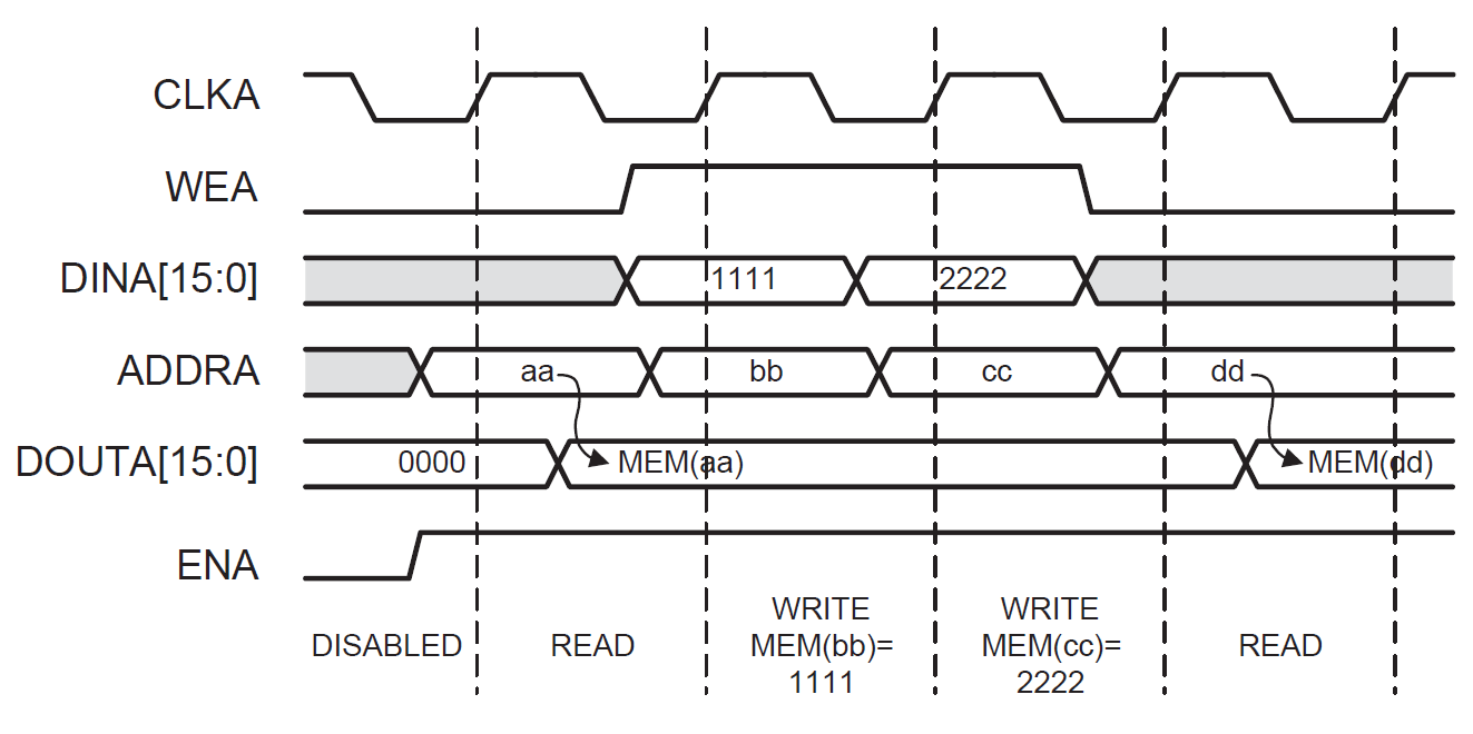
No Change Mode: 읽고 쓰기가 동시 에 이루어질 때 쓰기 바로 전 읽기만 했을때의 결과값을 유지시킨다.
In NO_CHANGE mode, the output latches remain unchanged during a Write operation.
Memory Output Flow Control

Assumtion
• That both output registers are used for port A
• The port A reset value is 0xFFFF
• En and regce are always asserted
• The block RAM embedded register is labeled REG1
• The output of the last register is the output of the core, dout.
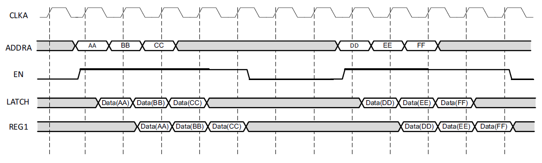
순서
1. ADDRA 주소의 데이터를 LATCH
2. Block Ram에 내장된 REG1에 LATCH 데이터 저장
3. DOUT으로 출력
• Addr 입력 후 3클럭 뒤에 데이터가 DOUT으로 출력
• 만약 RST가 High면 FFFF 출력 (Reset값)

• Only the memory primitive registers are used for port A,
• The data on the block RAM memory
• latch is labeled latch the block RAM embedded register, is the core output, dout.
• En is always asserted
• Rst is always deasserted
• 만약 REGCE가 1이면 현재 LATCH값 출력, 0이면 이전 LATCH값 유지
Read Data and Read Enable Latency
Assumtion
• There are no output registers
• The LATCH signal is the data at the output of the primitive.
1클럭 뒤에 데이터 출력

Assumtion
• The read data (REG1) and read enable (en) latency when the primitive output register is used.
Assumtion
• The read data (REG2, REG3) and read enable (en) latency when two pipeline stages are used along with the primitive output register.
• REG2 is the data at the output of the pipeline stage 1, and REG3 is the data at the output of the pipeline stage 2.
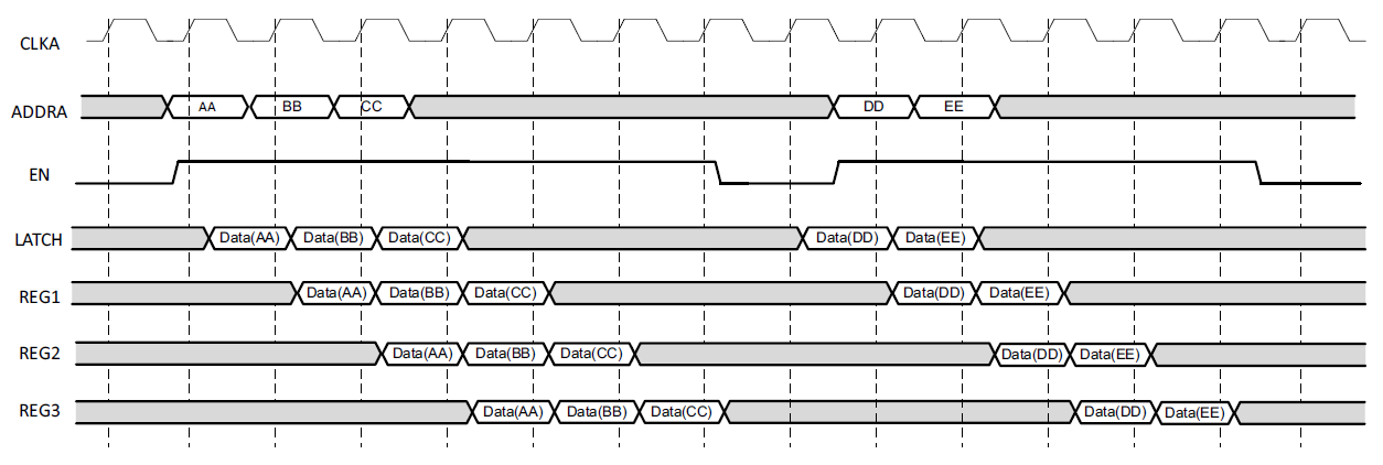
Assumtion
• The read data (dout) and read enable (en) latency when the core output registers are used along with the primitive output register and two pipeline stages.
• dout is the data at the output of the core output register.

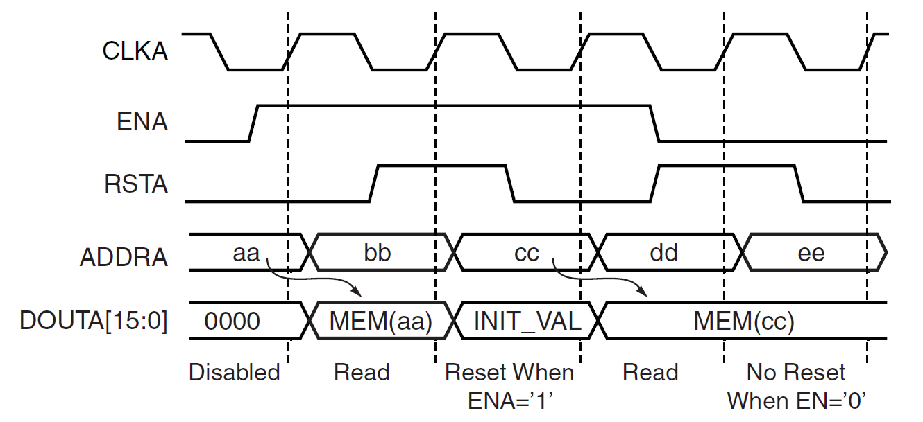
Reset Priority
Assumtion
• The Reset Priority option is set to CE
첫번째 RSTA가 assert 시 DOUTA[15:0]이 INIT_VAL로 초기화됨
반면에 두번째 RSTA가 assert시 ENA가 low에 있기때문에 초기화가 되지 않음
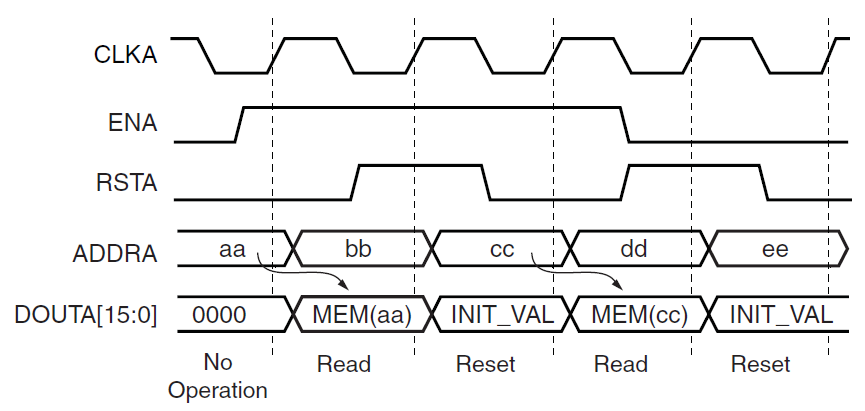
Assumtion
• The Reset Priority option is set to SR.
ENA에 관계없이 첫번째, 두번째 RSTA가 asset시 초기화됨
'FPGA > 개발' 카테고리의 다른 글
| [Xilinx FPGA, verilog] power-on reset을 하지 않았을 때 reg의 값은 무엇일까? (0) | 2022.05.30 |
|---|---|
| [Simulation] AXI read write tasks (0) | 2022.04.05 |
| [Vivado 2020.2] Block design내 hierarchy 시뮬레이션 방법 (0) | 2022.03.07 |
| [Vivado 2020.2] Subblock design (Hierarchy)를 다른 Vivado 프로젝트로 복사 방법 (0) | 2022.02.24 |
| Vitis 사용법 (0) | 2022.02.22 |


